DSD-4.1-memory
Memory
不同的方法来组织内存,如:ROM和RAM。
• Registers can store bits temporarily.
– But it is costly to use registers to store large amount of data.
– Key advantages of registers for data storage are speed and easy-of-use.
use memory storage devices to store data in higher density (capacity) and over longer time (volatility:断电也能保留存储内容).
Memory Sizes
内存大小通常使用2的幂来指定
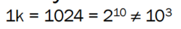
尽管通常在SI单位中使用10的幂

IEC -国际电工技术委员会-建议对2的幂使用单独的术语,以避免通信中的混淆。
General Model of Memory Device
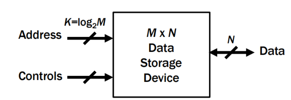
control用来控制读写或者电源
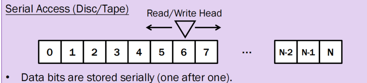
读/写头必须从当前位置传输到新地址,中间要经过其他地址,这很耗时。
适合于大量数据存储而不适合快速读写
Read/Write Memory
读/写内存(RWM)的特点是能够随时支持存储和检索
Most RWMs are random-access memory (RAM)
Most RAMs are volatile, meaning that they lose their memory when power is removed
Two main types:
– Static RAM (SRAM) – once word written at a location it remains stored until chip power removed or bit overwritten.
– Dynamic RAM (DRAM) – data stored at each location must be refreshed periodically by reading it and writing it back again or else it disappears.
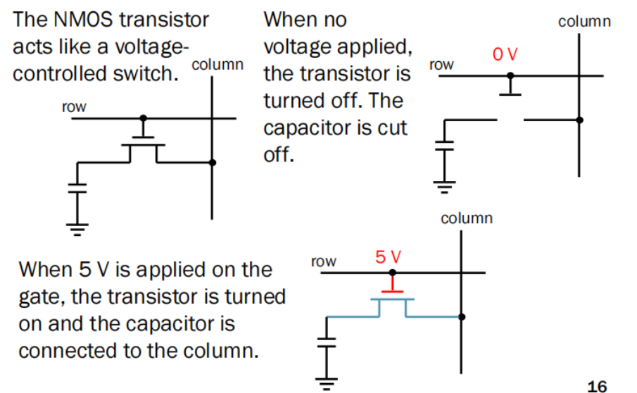
Dynamic RAM (DRAM)
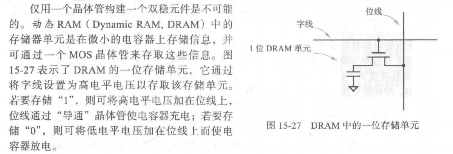
为了构建具有更高密度(每个芯片有更多比特)的ram,芯片设计师发明了每比特只使用一个晶体管的存储单元。基于dram的内存系统使用刷新周期定期更新每个内存单元。这涉及到将每个单元中有些退化的内容依次读入D-latch
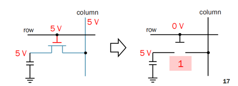
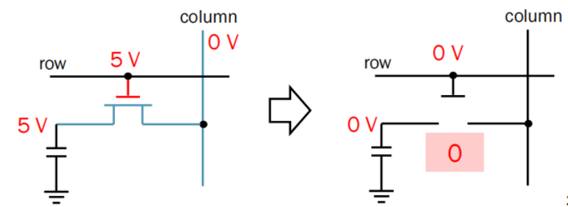
写5V(‘1’):先column设为5v,然后row设为5V, 最后等电容器电压到达5V后row设为0v
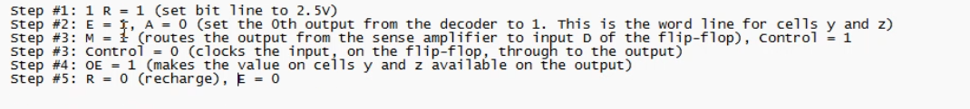
读取数据:

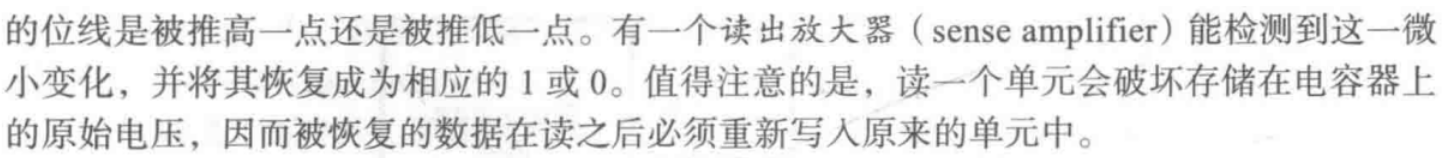

Bit line (i.e. column) is first pre-charged to a voltage half-wave between HIGH and LOW (e.g. 2.5 V).
A sense amplifier detects this small change and recovers a ‘1‘ or ‘0’, respectively
• set column to 2.5 V
• assert row to turn transistor ON
• sense voltage raise ‘1’ stored; otherwise ‘0‘
• bit latched
• write back: set column = Q
• output data OE = ‘1’
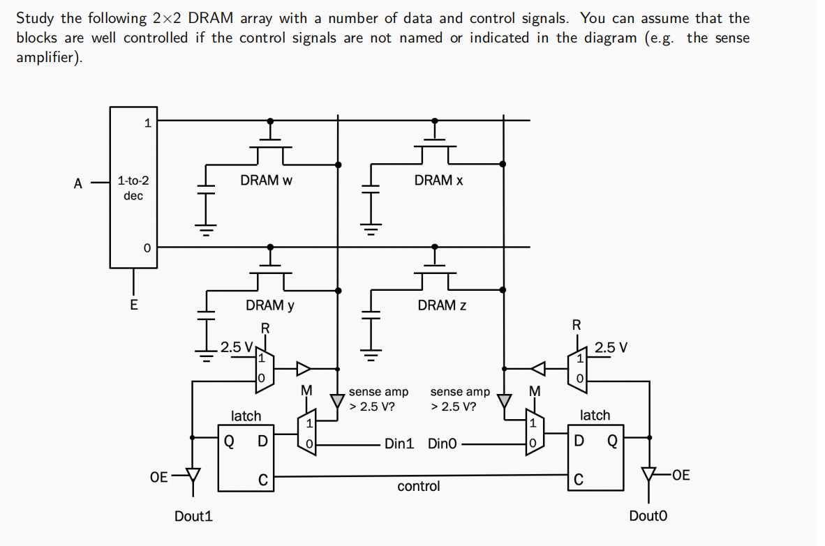
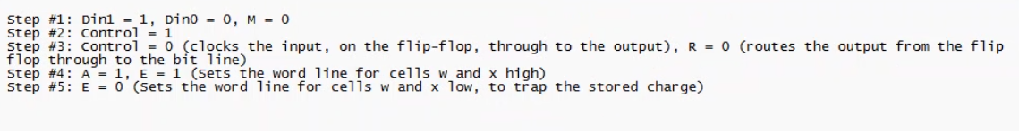
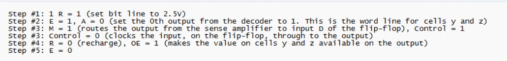
Write down the sequence of data and control signals to
write “10” to cells w and x;
read cells y and z;
copy cells y and z to cells w and x