DSD-2.3-Combinational Blocks
Combinational Blocks
基本门电路符号:
AND: 
OR: 
NO: 
NAND:
NOR: 
XOR(异或门):  相同为0 不同为1
XNOR(同或门):  相同为1 不同为0
Hierarchical Design
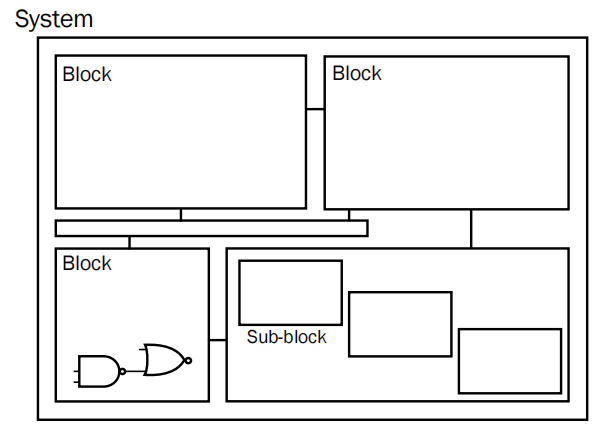
• The system is broken into pieces called blocks.
• Blocks are then interconnected to form the circuit.
– Functions and interfaces must be well defined.
Top-Down vs Bottom Up
• Top-Down Approach
– Study high-level specification/requirement
– Break the whole system into sub-systems
– Identify usable blocks/modules for the sub-systems
– Implement and link sub-systems
• Bottom-Up Approach
– Design flexible and reusable blocks/modules
– Map blocks/modules to common problems
– Prepare a category of useful cores (e.g. processing, communications)
– Pick and connect cores for different applications
Digital Data: Terminology
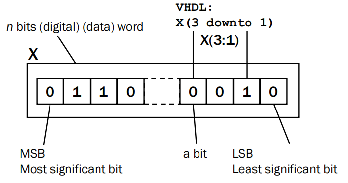
4 bits is a nibble(半字节); 8 bits is a byte
Combinational Circuits
Logic circuits for digital systems can be combinational and sequential
Combinational circuit has its outputs at any time determined only by the inputs (i.e. has no memory 不含有记忆原元件).
outputs = f(inputs)只与当前时刻输入有关,与过去输入无关
Sequential circuit contains element that store bit values (i.e. has memory 有记忆元件).
outputs = f(inputs, current_states) (输出方程)与输入变量和存储电路状态有关
next_states = f(inputs, current_states) (状态方程)
(Binary) Decoder
二进制译码器:输入m=2^n
A binary code of n bits is capable to representing up to 2^n distinct elements
n位二进制数可以最多表示2^n个数
converts binary inputs to a maximum of 2^n unique outputs
A common method to name decoders is by listing the no. of inputs and outputs: n-to-m-line decoders, e.g. 2-to-4-line decoder, 3-to-8 line decoder, etc.
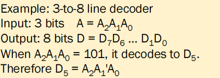
3-8 decoder
高电平有效(无enable)
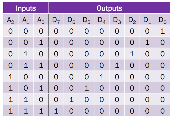
The function at each output of the decoder is just a minterm of the inputs.
输出是输入的各种组合:一个输出对应一个最小项
example: D0 =A2’A1 ‘A0 ‘ D1 = A2 A1’A0
entity decoder_3_8 is
port ( A : in std_logic_vector(2 downto 0); --2是高位
       D : out std_logic_vector(7 downto 0)); --7是高位
end decoder_3_8;
architecture decoder_3_8_arch of decoder_3_8 is
begin
    D <= "00000001" when A = "000" else
         "00000010" when A = "001" else
          …
         "01000000" when A = "110" else
         "10000000";
end decoder_3_8_arch;
Decoder with Enable
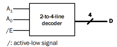
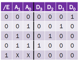
/E( 加/低电平有效?) :低电平有效(active-low):The decoder is enabled when /E = 0 (active-low), otherwise all outputs are ‘0’.
architecture dataflow_arch of decoder_2_4_en is
begin
    D <= "0001" when A = "00" and nE = '0' else
    "0010" when A = "01" and nE = '0' else
    "0100" when A = "10" and nE = '0' else
    "1000" when A = "11" and nE = '0' else
    "0000"; -- nE = '1
end dataflow_arch;
Decoder Expansion
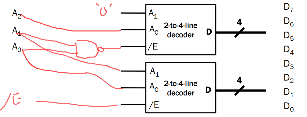
How to construct a 3-to-8 decoder with two 2-to-4 decoders with enable ?
Binary Encoder
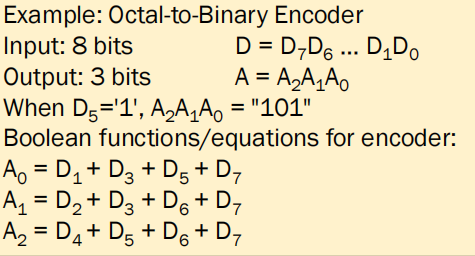
• An encoder performs the inverse operation of a decoder
It has 2^n input lines and n output lines
把2^n个输入转化成n个binary输出
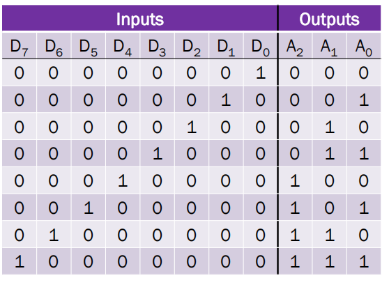
Output is the binary code of the corresponding input line
Assumption: only one input has a value ‘1’ at any time(非优先)
• When-else / With-select statement
entity encoder_8_3 is
port ( D : in std_logic_vector(7 downto 0);
       A : out std_logic_vector(2 downto 0));
end encoder_8_3;
architecture arch of encoder_8_3 is
begin
    A <= "000" when D="00000001" else
         "001" when D="00000010" else
         "010" when D="00000100" else
         "011" when D="00001000" else
         "100" when D="00010000" else
         "101" when D="00100000" else
         "110" when D="01000000" else
         "111" ;
end arch;
• Boolean equations
entity encoder_8_3 is
port ( D : in std_logic_vector(7 downto 0);
       A : out std_logic_vector(2 downto 0));
end encoder_8_3;
architecture arch of encoder_8_3 is
    A(0) <= D(1) or D(3) or D(5) or D(7);
    A(1) <= D(2) or D(3) or D(6) or D(7);
    A(2) <= D(4) or D(5) or D(6) or D(7);
begin
end arch;
Priority Encoder
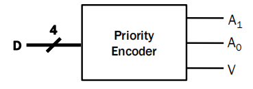
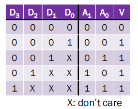
• Inputs are given different priorities, e.g. D3 > D2 > D1 >D0.
• Input having highest priority is encoded first.
• Easy implementation A1 = D3 + D2 , A0 = D3 + D2 ‘D1
V=valid(判断输出是否有效)高电平有效
Multiplexer (MUX) / Data Selector

多路复用器
• A multiplexer is a combinational circuit that selects binary information from one of many input lines and directs the information to a single output line
- It acts like a switch, though it repeats the logic value from the input.
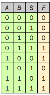
a 2-to-1 MUX selects one of its two inputs A or B to the output F based on the value at S.
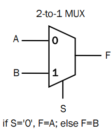
Boolean equation: F = S‘A + SB
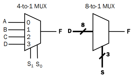
VHDL: 4-to-1 MUX
port ( D: in std_logic_vector(3 downto 0);
       S: in std_logic_vector(1 downto 0);
       Y: out std_logic);
end mux4;
architecture arch_mux4 of mux4 is
begin
    Y <= D(3) when (S = "11") else
    D(2) when (S = "10") else
    D(1) when (S = "01") else
    D(0) when (S = "00") else
    '0';
end arch_mux4;
Reminder: double quotes (“xxx”) for multiple signals / bus, single quote (‘y’) for a single signal / bit
entity mux4_8 is
port ( D3, D2, D1, D0: in std_logic_vector(7 downto 0);
      S : in std_logic_vector(1 downto 0);
      Y : out std_logic_vector(7 downto 0)
);
end mux4_8;
architecture arch of mux4_8 is
begin
    with S select
       Y <= D3 when "11",
       D2 when "10",
       D1 when "01",
       D0 when others;
end arch;
MUX Expansion
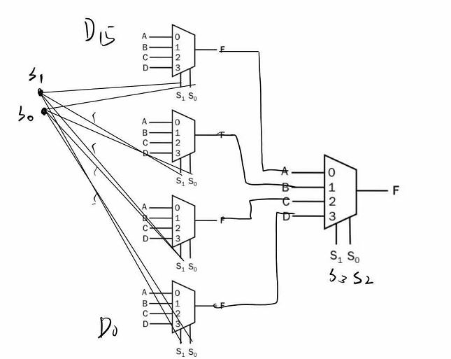
entity mux16 is
port ( D: in std_logic_vector(15 downto 0);
       S: in std_logic_vector(3 downto 0);
       Y: out std_logic);
end mux16;
architecture arch of mux16 is
component mux4 is
port (D: in std_logic_vector(3 downto 0);
      S: in std_logic_vector(1 downto 0);
      Y: out std_logic);
end component;
signal X: std_logic_vector(3 downto 0);
begin
     L1_M3: mux4 port map (D(15 downto 12), S(1 downto 0), X(3));
     L1_M2: mux4 port map (D(11 downto 8), S(1 downto 0), X(2));
     L1_M1: mux4 port map (D( 7 downto 4), S(1 downto 0), X(1));
     L1_M0: mux4 port map (D( 3 downto 0), S(1 downto 0), X(0));
     L2_M1: mux4 port map (X, S(3 downto 2), Y);
end arch;
计算selection signal的 no. =log2(no. of inputs)
Shifting
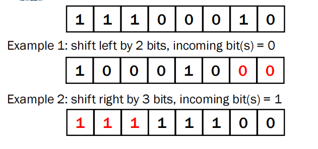
A word can be shifted left(right): the bits move towards MSB(LSB) side by a number of bits. New bits (incoming bits) are then shifted in to fill the empty bits.
Shifter is actually can be realised without any logic gate. The bits are aligned with the incoming bits as outputs.
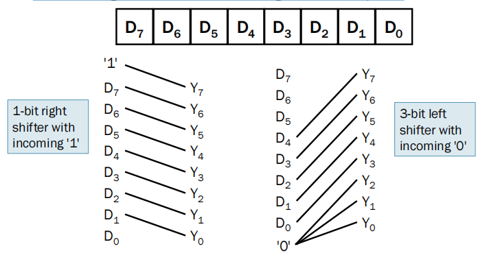
Barrel Shifter
Barrel shifter can shift a data word by a number of bits. It is combinational: contains MUX to choose the shifted bits as the outputs
e.g. design a 4-bit barrel shifter that can shift a 4-bit word 0, 1, 2 or 3 bits to the left with incoming bits as ‘0’. 四位的barrel shifter可以移动0,1,2,3位(通过控制信号可以调节不同的位数)
n比特数据的桶式移位器,需要的数据选择器数量为n比特数据的桶式移位器,需要的数据选择器数量为
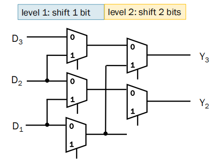
level 1:一次移动一位
level 2:一次移动两位
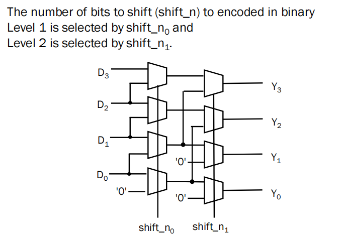
shift_n0 控制level 1是否移动
shift_n1控制level 2是否移动
entity barrel4 is
port ( D: in std_logic_vector(3 downto 0);
       shift_n: in std_logic_vector(1 downto 0);
       Y: out std_logic_vector(3 downto 0));
end barrel4;

architecture arch of barrel4 is

component mux2 is
port (A, B, S: in std_logic; -- Y <= A when S = '0' else B;
      Y: out std_logic);
end component;

signal D1, D0, X1, X0: std_logic_vector(3 downto 0);
begin
    MUX2_GEN: for i in 3 downto 0 generate
    L1: mux2 port map (D0(i), D1(i), shift_n(0), X0(i));
    L2: mux2 port map (X0(i), X1(i), shift_n(1), Y(i));
end generate MUX2_GEN;
    D0 <= D;
    D1 <= D0(2 downto 0) & '0'; -- shifted bits level 1 利用&将字节拼起来
    X1 <= X0(1 downto 0) & "00"; -- shifted bits level 2
end arch;
Binary Addition and Adders
Adder is the device to add two arithmetic operands (in binary) to give a sum (also in binary).
In addition, in order to handle subtraction, we just need a simple circuit to negate the operand (A – B → A + (-B)) and use the same adder.
Half Adders
输入:X、Y
输出:carry out 和 half sum

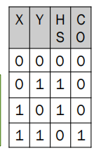
在此基础上加CIN构成full adder
Full Adders (FAs)
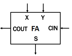
Specification:
Three 1-bit inputs – X, Y & CIN;
Two 1-bit outputs – S & COUT
{COUT, S} = X + Y + CIN

Ripple Adder
可以进行有符号的加分
行波进位加法器(用FA构成)
cascade adders to form a bigger adder to handle a N-bit addition
• The carry to the LSB is normally cleared (i.e. c0=’0’)
• Ripple adder is a classic example of an iterative circuit.

ripple adder is simple but slow since in the worse case c0 propagates all the way to c4
entity my_ripple_adder is
port ( X, Y : in std_logic_vector(3 downto 0);
       S : out std_logic_vector(3 downto 0);
       COUT : out std_logic);
end my_ripple_adder;
architecture my_ra_arch of my_ripple_adder is
    signal C: std_logic_vector(3 downto 0);
begin
    C(0) <= '0'; -- no carry in for LSB
    C(1) <= (X(0) and Y(0)) or (X(0) and C(0)) or (Y(0) and C(0));
    C(2) <= (X(1) and Y(1)) or (X(1) and C(1)) or (Y(1) and C(1));
    C(3) <= (X(2) and Y(2)) or (X(2) and C(2)) or (Y(2) and C(2));
    COUT <= (X(3) and Y(3)) or (X(3) and C(3)) or (Y(3) and C(3));
    S <= X xor Y xor C;
end my_ra_arch;
Ripple Adder with Port Maps
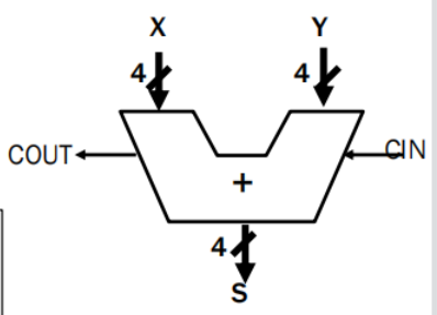
Step 1: Generate top-level entity declaration
entity my_ripple_adder is
port ( X, Y : in std_logic_vector(3 downto 0);
       CIN : in std_logic;
       S : out std_logic_vector(3 downto 0);
       COUT : out std_logic);
end my_ripple_adder;
Step 2: Declare the lower-level design units used
component FA is
port (X, Y, CIN: in std_logic;
      S, COUT : out std_logic);
end component;
Steps 3&4: Declare internal signals and create instances (port maps)
architecture structural of my_ripple_adder is
    component FA is
    port (X, Y, CIN: in std_logic;
          S, COUT : out std_logic);
    end component;
    signal C: std_logic_vector(3 downto 0);
begin
    I0: FA port map (X=>X(0), Y=>Y(0), CIN=>CIN, S=>S(0),  COUT=>C(1));
    I1: FA port map (X=>X(1), Y=>Y(1), CIN=>C(1), S=>S(1), COUT=>C(2));
    I2: FA port map (X=>X(2), Y=>Y(2), CIN=>C(2), S=>S(2), COUT=>C(3));
    I3: FA port map (X=>X(3), Y=>Y(3), CIN=>C(3), S=>S(3), COUT=>COUT);
end structural;
generate statement:
    signal C: std_logic_vector(4 downto 0);
begin
    FA_map_gen:
    for i in 0 to 3 generate
        INST: FA port map(X=>X(i), Y=>Y(i), CIN=>C(i),
                          S=>S(i), COUT=>C(i+1));
    end generate FA_map_gen;
    C(0) <= CIN;
    COUT <= C(4);
end structural;
Subtractor
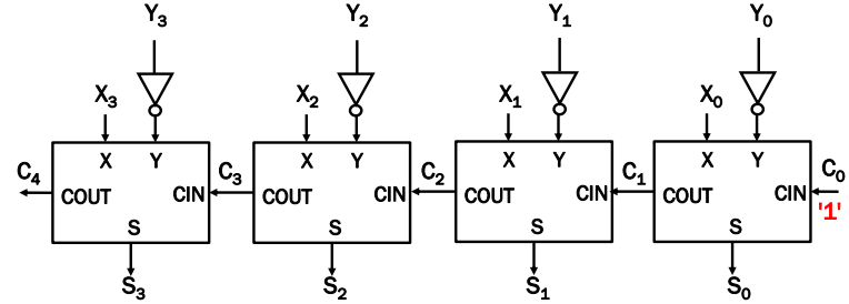
{2’s complement of Y} = Y’ + 1 (Y’ is bitwise NOT/complement)
c0=1 代表着 Y’+ 000..01
entity my_ripple_subtractor is
port ( X, Y : in std_logic_vector(3 downto 0);
       S : out std_logic_vector(3 downto 0);
       COUT : out std_logic);
end my_ripple_subtractor;
architecture my_rs_arch of my_ripple_subtractor is
    signal C, Yn: std_logic_vector(3 downto 0);
begin
    Yn <= not Y;
    C(0) <= '1'; -- extra '1' for 2's complement
    C(1) <= (X(0) and Yn(0)) or (X(0) and C(0)) or (Yn(0) and C(0));
    C(2) <= (X(1) and Yn(1)) or (X(1) and C(1)) or (Yn(1) and C(1));
    C(3) <= (X(2) and Yn(2)) or (X(2) and C(2)) or (Yn(2) and C(2));
    COUT <= (X(3) and Yn(3)) or (X(3) and C(3)) or (Yn(3) and C(3));
    S <= X xor Yn xor C;
end my_rs_arch;
Auto-Synthesis of Adders
In many design tools, adders can be described using the ‘+’ operator. (‘-‘ for subtractor).
an appropriate adder will be implemented automatically
it will try to choose an implementation that best fits the target device
-- unsigned 8-bit adder/subtractor
library IEEE;
use IEEE.std_logic_1164.all;
use IEEE.std_logic_unsigned.all;
entity adder_7 is
port ( A, B : in std_logic_vector(7 downto 0);
       OPER : in std_logic;
       SUM : out std_logic_vector(7 downto 0));
end adder_1;
architecture archi of adder_7 is
begin
    SUM <= A + B when OPER = '0' else
           A - B;
end archi;
You describe an adder and a subtractor for operands A and B and choose between sum and difference by an input OPER.
Arithmetic Logic Unit (ALU)
An arithmetic and logic unit (ALU) is a combinational circuit that can perform any of a number of different arithmetic and logical operations on a pair of N-bit operands
The operations is chosen by a function-select inputs.
it is simply a list of circuits whose outputs selected by a MUX.
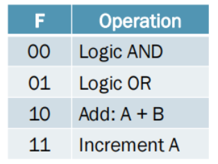
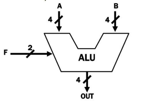
4-bit AND gate and a 4-bit OR gate, a 4-bit ripple adder for addition and increment.
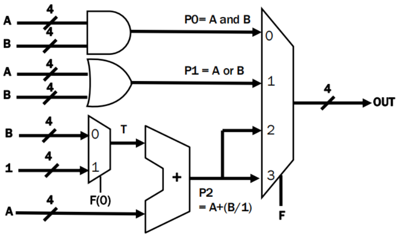
architecture simple_alu_arch of simple_alu is
    signal P2, P1, P0, T: std_logic_vector(3 downto 0);
begin
    -- 4-bit AND gate and OR gate
    P0 <= A and B;
    P1 <= A or B;
    -- 2-to-1 MUX
    T <= B when F(0) = '0' else "0001";
    -- Auto-adder
    P2 <= A + T;
    -- MUX 4-to-1
    OUT <= P2 when (F = "11") else
           P2 when (F = "10") else
           P1 when (F = "01") else
           P0 when (F = "00") else '0';
end simple_alu_arch;
Bit-Slicing the ALU
ALU位数切分
entity ALUSlice is
port (
   A, B: in std_logic;
   K, CIN: in std_logic;
   F: in std_logic_vector(1 downto 0);
   OUT, COUT: out std_logic);
end ALUSlice;
create a bit-slice circuit that handles operation for a bit of the operands, e.g. A(0) vs B(0). (每位的ALU)
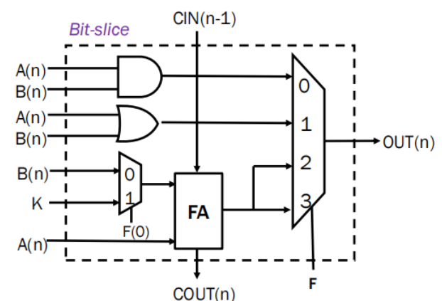
we can cascade N slices together to form a N-bit ALU.
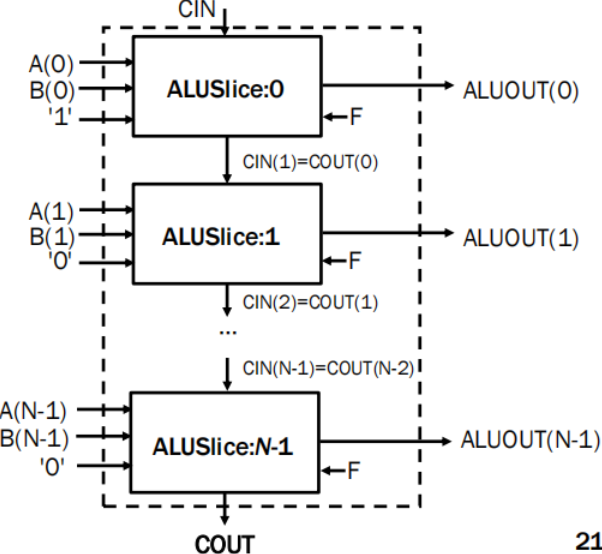
最低位的slice输入‘1’其余为‘0’ 因为加1操作实际上加00…01


