DSD-2.4-Sequential Building Blocks
Sequential Building Blocks
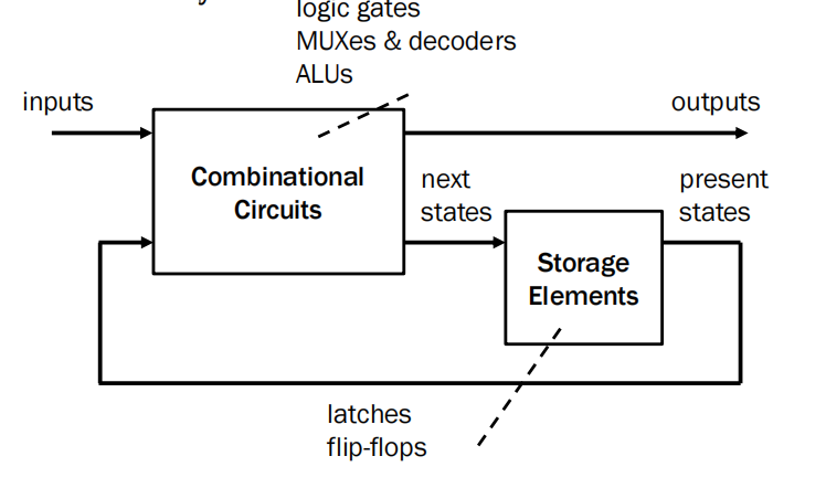
Sequential Circuits
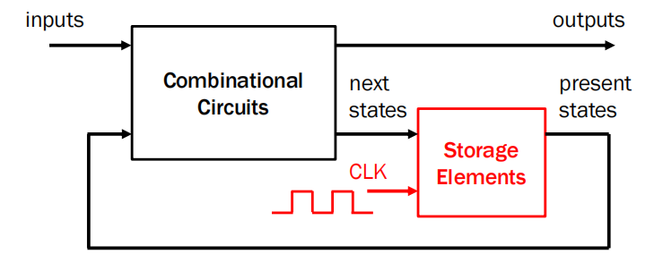
Sequential circuits consist of combinational circuits and some form of memory.
(组合电路+记忆元件)
记忆元件:锁存器和触发器
Synchronous System
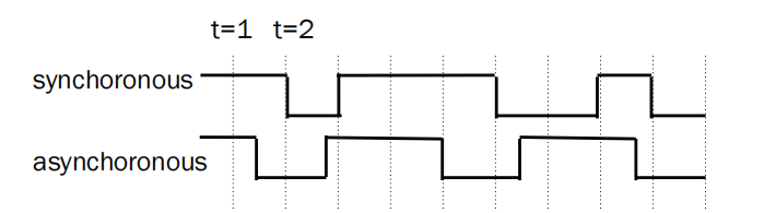
synchronous: If a sequential circuit has its behavior/outputs changed at discrete moments in time, then it is said to be synchronous(只在特定点更改行为)
asynchronous: If the outputs can change at any instant of time, it is called asynchronous
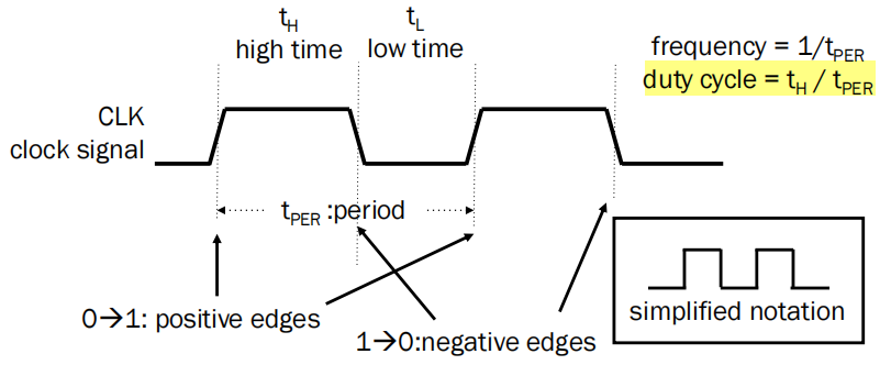
Clock Signal
We can use a signal shared by all storage elements for synchronisation – to ensure that each of them to change its output (if any) only at desired moments of changes.
两种Storage Elements与CLK有关
latches and flip-flops (FF):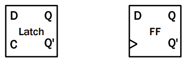
锁存器与触发器区别:
锁存器(latch)在电平信号的作用下改变状态,是一种对脉冲电平(即0或者1)敏感的存储单元电路(Sensitive to pulse level (i.e., 0 or 1))。锁存器的数据存储动作取决于输入使能信号的电平值,仅当锁存器处于使能状态时,输出数据才会随着数据输入发生变化,否则处于锁存状态。
触发器(Flip-Flop,简写为 FF)是一种对脉冲边沿(即上升沿或者下降沿)敏感的存储电路(It is sensitive to the edge of the pulse (i.e. the rising edge or falling edge))。随着输入的变化,输出会产生对应的变化。它通常是由至少两个相同的门电路构成的具有反馈性质的组合逻辑电路。应用中为了使触发过程容易控制,而做成由时钟触发控制的时序逻辑电路。
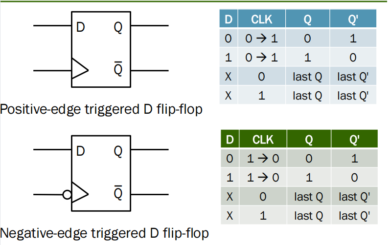
D Latch
inputs: Data (D) and Control (C)
Its output Q follows D when C = ‘1’
otherwise Q remains unchanged.
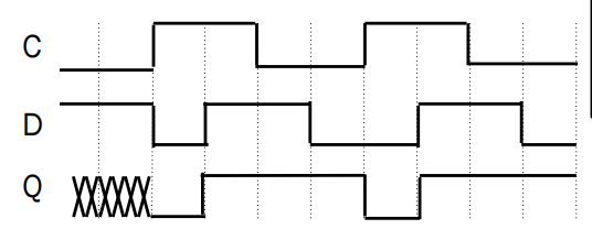
当c=0时,Q保持不变,即锁存。
Master-Slave D Flip-flop
D flip-flop is a very important sequential component which can be synchronised at clock edges.
use two latches to isolate output of the flip-flop from its input(用两个锁存器把输入输出隔离开,当主latch工作时候,slave latch出于锁存状态,当达到上升沿才解除锁存状态,把X传到Q)
Master-slave flip-flop: master latch holds input at an internal node and the slave latch holds the internal node (X) to output
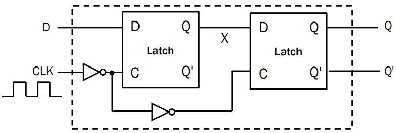
CLK = ‘0’:
master latch is ON, X = D; slave latch is OFF, Q unchanged.
CLK = ‘1’:
master latch is OFF, X unchanged; slave latch is ON, Q = X
Overall effect: Q gets value of D when CLK changes from 0 to 1
D Flip-flop
用behavioural models去描述FF ,而不是去用 concurrent statement去描述。
architecture my_d_ff of d_ff is
begin
    dff: process (CLK)
    begin
        if (CLK'event and CLK = '1') then -- rising_edge(CLK)
            Q <= D;
        end if;
    end process dff;
end my_d_ff;
CLK’event means a 0 to 1 or 1 to 0 transition.
Additional CLK=’1’ implies we want a rising edge (0 to 1).
It is important that you intentionally omit a signal assignment outside the if statement.
省略之后代表不改变当前输出 这其中implying a D flip-flop
The cryptic method of designing sequential circuit in VHDL
设计时序电路的隐式规则:
combinational:signal always has an assignment after execution of all sequential statements
sequential: otherwise(少写一个if) memory element like D flip-flop is needed to keep the old value
如果代码不是涉及到所有情况,synthesiser就会自动生成一个latch。
但是现在数字设计中很少使用latch
So you’d better check your codes to make sure you provide a default signal assignment or a catch-all condition.
architecture arch of entity1 is
    signal S, A, B: std_logic;
begin
    latch_ex: process (A, B)
    begin
        if (A = '1') then
            S <= '1';
        elsif (B = '1') then
            S <= '0';
        end if;
    end process latch_ex;
end arch;
how about the remaining cases?VHDL assumes to keep value of S, so a latch is required.
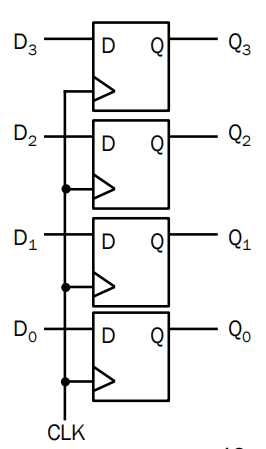
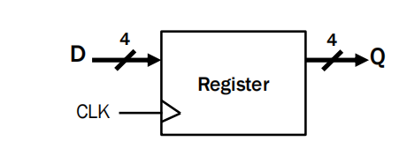
Register
we group a set of D flip-flops to store a word, it is called a register
Loadable Registers
可加载的寄存器(使用一个MUX在新数据和原始数据间选择)
The idea is to use a MUX to pick between the new data DN or the original data QN . Imagine this structure is expanded for N bits.
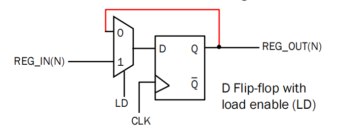
A loadable register can therefore be built using a number of D flip-flops with enable.
entity reg8 is
port ( REG_IN: in std_logic_vector(7 downto 0);
       LD, CLK: in std_logic;
       REG_OUT: out std_logic_vector(7 downto 0));
end reg8;
architecture reg8_arch of reg8 is
begin
    reg: process (CLK)
    begin
        if (CLK'event and CLK = '1') then
            if (LD = '1') then
                REG_OUT <= REG_IN;
            end if;
        end if;
    end process reg;
end reg8_arch;
There is no else statement, inferring 8 D flip-flops
It is good and recommended to separate the CLK and LD signals to make a clear inferring of component(最好把CLK和LD分开)
Shift registers & Counters and their applications.
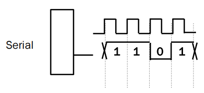
Serial vs Parallel
(书上有,记得看)
There are two main ways to present a input (N bits) to a system:
Serial: one bit is presented per cycle (N clock periods required)
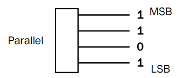
Parallel: N bits together at a cycle (1 clock period required)
Shift Register
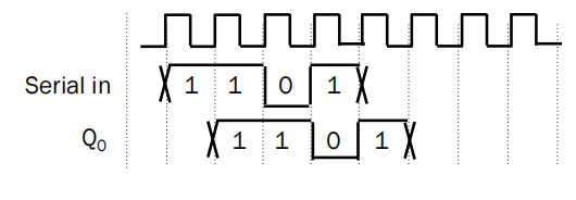
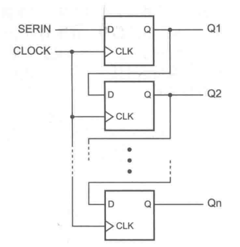
We can cascade a number of D flip-flops sharing the same clock to construct a shift register.
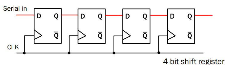

每个时钟到来都会把数据向前移动一位
因为从CLK上升沿到来到输出端新状态的建立还需要一段时间的传输延时,所以当clk上升沿同时作用于所有触发器时,它们的输入端的输入信号为前一个触发器原来的输出状态,即维持时钟到来前的状态。总的效果相当于所有代码向右移动了一位0
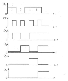
如图当第一个cp上升沿到达时只有Q0变化,第二个上升沿是Q0,Q1都变化….直到四个clk信号后串行输入的四位全部转入寄存器,四个触发器的输出端此时可以得到四个并行输出
Serial to Parallel Conversion
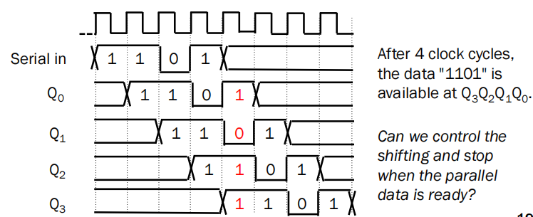
可以看出中间红色为串行输入的并行输出,所以串并转换的寄存器只需要每一级都有输出
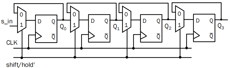
Shift Register with Output Hold
Use a MUX to choose between shift input and original output.
(This is the same as using D flip-flop with enable)
shift/hold’ = 1: shift s_in through the shift register
shift/hold’ = 0: keep the current data and stop shifting
entity ShiftRegHold is
port (CLK, HOLDn : in std_logic;
      S_IN : in std_logic;
      Q : out std_logic_vector(3 downto 0));
end ShiftRegHold;
architecture beh of ShiftRegHold is
    signal S, Qint, D: std_logic_vector(3 downto 0);
begin
    Q <= Qint; -- mirror to output
    reg: process (CLK)
    begin
        if (CLK'event and CLK = '1') then
            Qint <= D;
        end if;
    end process;
    D <= Qint when HOLDn = '0' else S; -- 2-to-1 MUX
    S <= Qint(2 downto 0) & S_IN; -- shifted bits
end beh;
注意S_in 是一位信号
由于Q是一个输出信号不能直接读取,而且我们不知道Q初始值是啥,设一个Qint作为初始值赋值给Q,再对Qint 进行移位。
Parallel to Serial Conversion
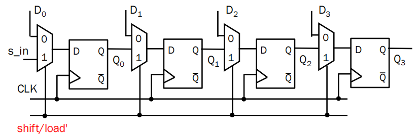
shift/load’ = 1: shift s_in through the shift register
shift/load’ = 0: load parallel value from input bus D
So far the direction of shifting is fixed (shift right to the diagram, but literally left Q3Q2Q1Q0 )
Universal Shift Register
Let’s build a bit slice for a universal shift register: hold, load, shift left and shift right
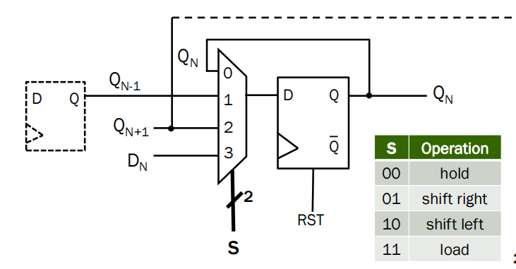
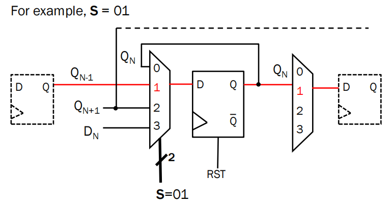
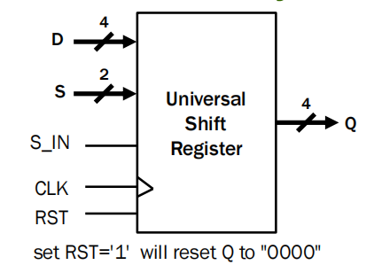
entity UnivShiftReg is
port (D : in std_logic_vector(3 downto 0);
      CLK, RST : in std_logic;
      S: : in std_logic_vector(1 downto 0);
      S_IN : in std_logic;
      Q : out std_logic_vector(3 downto 0));
end UnivShiftReg;
Counter
A counter is a circuit that counts (in binary): 0, 1, 2
It has to be sequential in nature since memory storage is necessary to keep the value of count
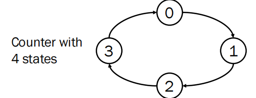
模M计数器: a counter with M states is called a modulo-M counter.
因为 it can be used to calculate (N mod M)
Ripple Counter
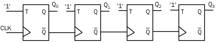
- General structure: Each T (toggler) flip-flop is clocked by the rising edge of the previous Q’ output (i.e. the falling edge of Q).
这里使用T触发器:在T=1时,时钟每个上升沿Q翻转
The frequencies are being divided by 2 as you go along Q0 , Q1 , Q2 , Q3 .
每输出一个Q 频率就会减小一半(周期扩大一倍)这是由于只在q bar 的上升沿(q的下降沿)变化所以周期会变大
频率越靠下越小
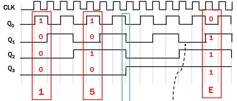
Effects of Delay
In reality, the logic gates and flip-flops have some propagation delays, so the changes are not immediate
640is propagation delay (output of Q0 Q1 Q2 are not synchronized)
Asynchronous
Ripple counter is asynchronous, since each flip-flop is clocked separately
You need to wait until the output becomes stable to read the correct results.
Therefore the clock frequency cannot be too high.
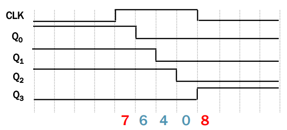
Synchronous Counters
Basic requirement: outputs change simultaneously(at/soon after the clock edge)
View the counter as adding 1 every clock So we can use (ripple) half adders to pre-calculate N+1, and then output N+1 using D flip-flops at clock edges.
理解为先全部加(00001)等一个时钟来全部输出到下一个状态的输入
We can derive an up counter as well as an up/down counter
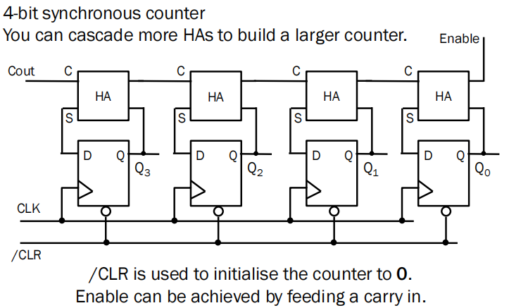
Suppose we now count to 5 “0101”, the HA chains will calculate “0101” + 1, giving “0110”, which is outputed at next clock edge.
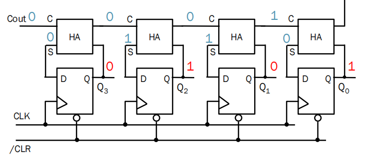
0101是现在状态,0101通过四个半加器后输出0110到D,然后等下个时钟到来时转移到q
可调加减的计数器的VHDL
entity CounterUpDown is
port (CLK : in std_logic;
      nCLR, UP: in std_logic;
      Q : out std_logic_vector(3 downto 0));
end CounterUpDown;
architecture arch of CounterUpDown is
    signal Qint: std_logic_vector(3 downto 0);
begin
    cnt_proc: process (nCLR, CLK)
    begin
      if (nCLR = '0') then
        Qint <= "0000";
      elsif (CLK'event and CLK = '1') then
         if (UP = '1') then
            Qint <= Qint + 1;
         else
            Qint <= Qint – 1;
         end if;
     end if;
  end process;
  Q <= Qint;
end arch;